TL;DR
A November 22, 2026 explainer uses 3D models to show how compute dies, high-bandwidth memory stacks and silicon packaging fit together in AI accelerators. Vendor specifications show rising memory bandwidth and increasingly complex packages, while SK hynix expects demand for memory to exceed supply through 2030; the scale of any resulting price or availability impact is not quantified.
Thorsten Meyer AI published a 3D explainer on November 22, 2026, showing how compute dies, stacked high-bandwidth memory (HBM) and advanced packaging combine inside AI accelerators. The report’s central point is that accelerator performance and supply depend on more than the processor: memory bandwidth and the capacity to package these components also matter.

Get the latest gadgets delivered free with Prime
- Fast, free delivery on millions of items
- Prime Video, Amazon Music and more included
- Member-only deals all year
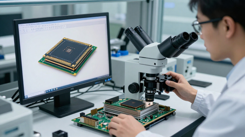
The model depicts a package with a substrate at its base, a silicon interposer carrying dense connections, compute dies and memory stacks, with a cold plate above for cooling. The source says the component order and counts follow vendor documents, but the sizes are schematic because the vendors do not publish dimensions for the dies, package or memory stacks.
The explainer compares different chip architectures rather than describing one universal design. Nvidia says its Rubin GPU uses two reticle-limited compute dies and has 336 billion transistors. AMD says its MI350 Series GPUs integrate eight vertically stacked accelerator complex dies and two I/O dies; the MI355X has 185 billion transistors and eight stacks of 12-high memory, according to the source’s account of AMD specifications.
HBM consists of DRAM layers joined vertically using through-silicon vias, or TSVs. The explainer cites Nvidia’s product page for memory bandwidth figures rising from 900 GB/s for V100 to 19.2 TB/s for Rubin. Those are vendor specifications for different products; the source does not provide a test comparing their performance on the same workload.

Packaging Limits Accelerator Supply
AI accelerators need to move data between compute and memory at high speed. Placing HBM close to the compute dies and connecting them through a silicon interposer lets a package carry many connections in a small area. This makes packaging part of the performance design, rather than a simple housing step.
The same complexity can constrain how many accelerators manufacturers can produce. The source cites SK hynix’s expectation that memory demand will exceed supply through 2030. That is a company forecast, not a measured guarantee of future shortages. The explainer does not quantify how much packaging capacity or memory supply will limit production, or how those constraints could affect prices for buyers.
Products Worth Considering

Jackery Solar Generator 1000 v2 with 200W Solar Panel, 1024Wh LiFePO4 Battery

Logitech MX Mechanical Wireless Illuminated Keyboard, Tactile Quiet, Graphite

Bose QuietComfort Ultra Wireless Noise-Cancelling Over-Ear Headphones with Spatial Audio, White Smoke
As an affiliate, we earn on qualifying purchases.
From Interposer to Rack
A reticle is the maximum area a chipmaking scanner can print in one exposure. TSMC says its CoWoS-S packaging can use a silicon interposer up to about 2,700 square millimeters, or 3.3 times reticle size. For larger packages, CoWoS-L joins smaller silicon bridges within a carrier layer. TSMC’s chief executive said on October 15, 2026, that the company was producing packages at five times reticle size and working on 9x and 14x designs, according to the source.
The report also follows the hardware outward to an AMD rack configuration: eight accelerator modules connect to a universal baseboard using Infinity Fabric. Its video and models draw on AMD’s CDNA 4 white paper, TSMC’s CoWoS information and Nvidia’s DGX GB user guide. The source credits Thorsten Meyer AI with creating the 3D models in SolidCraft and Blender, and says the narration uses an AI voice clone.
“large silicon interposer area to accommodate various functional top dies, including logic chiplets, with high-bandwidth memory (HBM) cubes stacked over it”
— TSMC, describing CoWoS-S
Dimensions and Supply Effects
The 3D model does not establish the physical dimensions of the depicted components: its sizes are schematic, and the source says vendors have not published those measurements. The report also does not provide an independent comparison of accelerator performance or a quantified estimate of manufacturing capacity.
How much packaging and memory constraints will limit shipments, and what they will mean for prices, remain unclear. SK hynix’s supply outlook is a company forecast. The source does not include a detailed methodology, broader industry estimates or a timeline for resolving any shortfall.
Capacity Expansion and New Packages
The next indicators will be whether memory makers and packaging suppliers expand output, and whether announced larger package designs move into production at scale. TSMC has said it is working on packages at 9x and 14x reticle size; AMD says its MI455X and MI450X use CoWoS-L and stacked 3D hybrid-bonded compute dies. The source gives no production dates for those AMD products or for the larger TSMC package designs, so their commercial availability remains to be seen.
Key Questions
What is HBM?
HBM, or high-bandwidth memory, is DRAM arranged in vertical stacks and connected with through-silicon vias. The stacked design places memory close to accelerator compute dies.
What does the silicon interposer do?
The interposer carries dense connections between compute dies and HBM stacks. The source describes it as a wiring layer inside the package.
Are the 3D model’s component sizes exact?
No. The source says the model’s sizes are schematic. Its layer order and component counts follow vendor documents, but dimensions are not provided.
Does the report confirm an AI chip shortage through 2030?
No. It reports SK hynix’s forecast that memory demand will exceed supply through 2030. That forecast does not establish the scale of a shortage or its effect on accelerator availability and prices.
Source: Thorsten Meyer AI